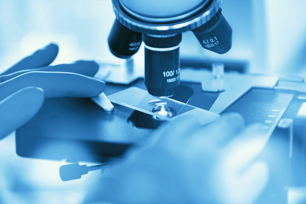
This development focuses on bringing together cutting-edge technologies for visualizing and analyzing nanoscaled structures that have direct applications in industry and research. Super-resolution techniques, such as STED, PALM, and STORM, overcome the diffraction limit, enabling resolutions down to 20 nm. This is essential for molecular cell biology and drug research. Live-cell nanoscopy builds on these capabilities by enabling real-time observation of dynamic processes in living systems. Photosafe procedures and optimized fluorophores minimize the invasiveness of cellular processes.
Integrating complementary techniques opens up new dimensions of analysis. For instance, combining atomic force microscopy (AFM) with Raman spectroscopy or fluorescence microscopy provides information about topography, chemical composition, and biological functionality simultaneously. In materials science, this allows for the precise characterization of two-dimensional materials, nanocomposites, and their interfaces.
Correlative nanoscopy workflows combine electron and light microscopy techniques to enable comprehensive structural analyses at scales ranging from micrometers to nanometers. AI-powered image analysis automates data analysis and pattern recognition, accelerating research processes and revealing hidden connections in complex datasets. This approach addresses critical challenges in medical technology, the semiconductor industry, and biotechnology, establishing new groundwork for innovative products and services in the nanoscience sector.
Development needs
- Miniaturization of nanoscopy on a chip for cost-effective, high-throughput applications.
- Multimodal sensor systems must be developed that combine optical, electrochemical, and mechanical detection principles.
- Machine learning algorithms must be integrated for real-time data analysis and pattern recognition.
- The development of maintenance-free, self-calibrating sensor systems is necessary for long-term measurements.